LNA Optimization. Some history The first time I made use of a noise generator was in 1963. I found a 2D2S vacuum noise diode and built my first instrument for measuring the noise factor. It was the vacuum tube era, although it was already coming to an end. The supreme achievement was the so-called Nuvistors, developed by RCA, which had the best noise parameters. Russia started to produce its own version of Nuvistors (e.g. 6S52N, 6S53N ...), but it was too late to get wide application. But even before this came the Soviet miniature metal-ceramic tube 6S17K which had very low noise that was even better than Nuvistors and long provided the best performance, not yielding even to the best of the transistors.
I built my first transistor receiver for 144 and 432 MHz in 1966. The input stages used the best experimental transistors but nevertheless, they were inferior to the tubes. Perhaps only in the 1970’s tubes were finally defeated. In the second half of the 70’s I finished the development of transistor transverters for three VHF/UHF bands (144 MHz, 432 MHz and 1296 MHz) and described it in a book. From the early 80s until the mid 90’s I was almost completely consumed with my work (QRL). When I returned to amateur radio I found there was a revolution in LNA technology with the appearance on the market of low-noise GaAs field effect transistors ( GaAs FET). These transistors redefined the limits of achievable performance and at room temperature it became possible to get results previously realized only by huge efforts at cryogenic temperatures. Over the past 10 - 20 years further improvements in the noise parameters are not as significant and now there is a feeling that the major technological advances are behind us at these low frequencies.
The amateur radio use of these transistors is not in the frequencies for which they are intended and even 1296 MHz is too low a frequency for most of them. Therefore, the first LNA's for UHF were very unstable. But that was 30 years ago and although I only started to study this topic four years ago, I was supported by all the previous experience in designing these amplifiers.
Of course, a good understanding of the various tricks necessary to create a good LNA did not come immediately. This only came after I had created a measurement setup with the "cold" horn antenna and had accumulated some experience through making several versions of LNA. By this time my attention was drawn to the VLNA by G4DDK. I liked this preamp at "first sight", because it was very close to my understanding of where my next step would be. The whole scheme, including the design was all pretty simple, with a box of tinplate, and a printed circuit board of conventional FR4 material. The input circuit has no contact with the PCB and is "hanging in the air" between the input connector and gate of the transistor in order to reduce the losses. Then it uses two stages which is not just what we need to obtain the necessary gain, it but it is also easier to ensure stability.
I copied the PCB from the picture and used a ATF36077 device for the first test. Quite easily I got the noise factor a little more than 0.3 dB. The only problem was a parasitic microwave oscillation that I had to to eliminate. Nevertheless my general impression was very good. All my later experiments were done on this "platform" and I was assisted by Vladimir RA3ACE, who assembled a few printed circuit boards for me, while I was busy with providing the boxes, connectors and the input transistors. This allowed me to do new tests and to work much faster. Now it was possible to make extra LNA's for use only as a "standard" to calibrate the measuring system. The main thing is that I was free from the need to think about stabilizers, DC converters, regulators etc (everything that I was usually too lazy or troubled to do). I was free to concentrate on the essentials and to fight for the best Noise Figure!
In this section I do not want to write formulas and delve into the theory, but just try to show the tricks I used to improve the sensitivity of LNA. These tricks have been found in numerous experiments by the method of trial and error. Of course this was made possible thanks to accurate and reliable measurements but of course these experiments were based on some basic principles and some hypotheses.
For a long time I looked for a way of showing the improvements made through changes and finally I decided to build the original version of the G4DDK VLNA and gradually make my own changes. After each change I have noted the result after giving the necessary illustrations and explanations. Fortunately some time ago I bought two kits from Sam G4DDK, one for my friend and one kit for myself and these kits are now very handy for this work. Step 1. Original version of VLNA by G4DDK.Assembling the LNA did not cause any problems. As always I paid special attention to assembling the input circuit. It is very important to carefully handle the solder flux. If rosin flux falls under the input transistor, it can significantly degrade the noise figure. The same applies to the input capacitor of 2.7 pF and the input connector. If flux gets into the gap between the central pin and PTFE insulator, it is hard work to remove it. It is not easy to determine the degree of NF degradation because I had no special experiments to show this, but the degradation of the noise figure was observed more than once. So it is better not to risk it. Finally I used a thin solder (0.25mm) for this work that contains little flux. The leads of the transistor are a bit bent, so that it slightly raised above the board. I tried to solder only the tips of leads to the ground plane. The same applies to the central pin of input connector. For this test I used gold plated connectors produced by Amphenol.
The first test of the LNA passed without surprises but the noise figure was worse than expected. I think it was about 0.35 dB or even worse. It turns out that there was an oscillation at higher microwave frequencies.
To confirm the oscillation I used a simple test method. I removed the cover of the amplifier and put my hand in 50...100 mm over the amplifier, and then moved my hand up and down while at the same time watching the level of noise on the screen of a spectrum analyzer. If moving my hand had no effect on this level then all was OK. If the level starts to fluctuate rapidly, microwave oscillation was there. For example, see Figure 4.1.
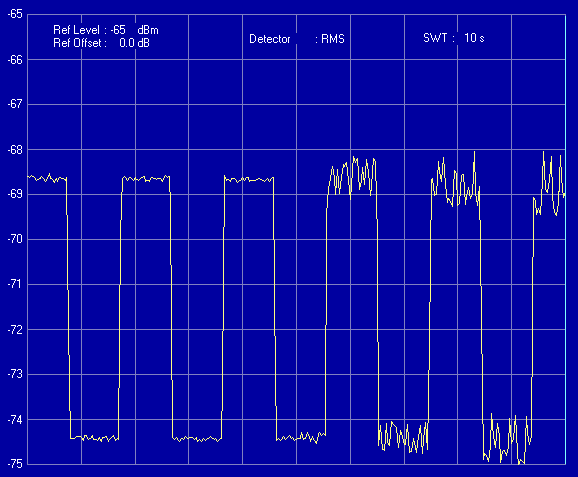 Fig. 4.1 Noise output of LNA during Unstable Operation
Here, the sweep time was 10 sec and for one half the time I held my hand motionless, the other half my hand was moving up and down. You can certainly do this testing without a spectrum analyzer. You can just look at the current of the input transistor. To experiment with this I connected an oscilloscope to resistor R4 (150 Ohm). I set the scope input to AC and set the sensitivity of 5 mV in the division. The influence of the oscilloscope probe is small and it is isolated from "ground". Therefore, I connected it directly parallel to resistor R4. In Figure 4.2 we can see that this measurement method also shows the instability.
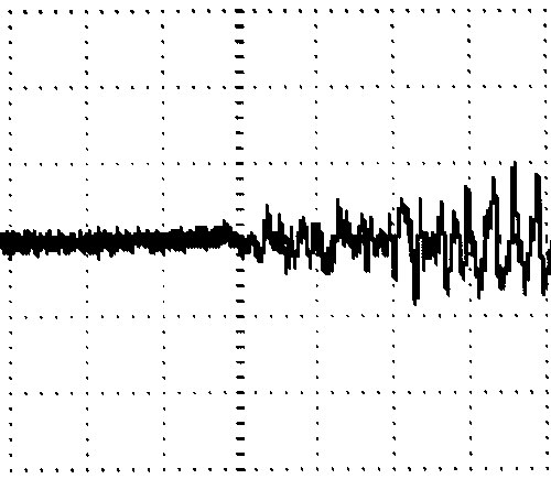 Fig. 4.2 Oscillation of DC current in LNA FET as seen with an Oscilloscope
I had to put a piece of the absorber near the output of the first stage as shown in Figure 4.3.
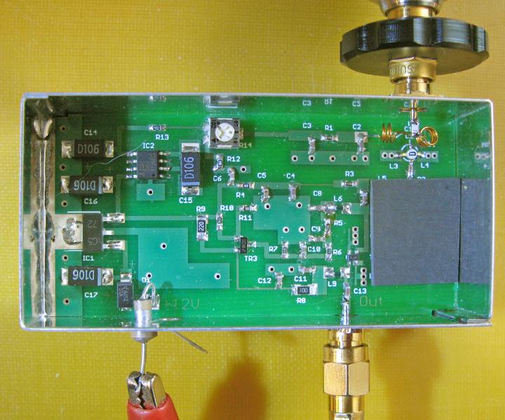 Fig. 4.3 LNA showing placement of 'Lossy Rubber' Absorber material
The oscillation completely disappeared. With tuning the bias voltage, the optimum gain corresponds to the maximum of noise signal at the output of LNA, ie, maximum gain. Then I tuned a bit L1 coil for best NF. The final result is shown in the screenshot of Figure 4.4.
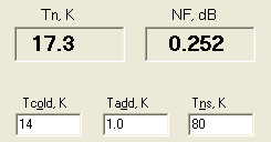 Fig. 4.4 Noise Figure Final Result Step 2. Optimization of the input stage.
The main problem with optimization is to get the best sensitivity while maintaining the stability of the LNA. Typically, these parameters contradict each other and we need to look for a compromise. For professionals the usual requirement is unconditional stability of the LNA. This means that the oscillation of the amplifier should be absent, regardless of conditions at the input and output for any load impedance (at any SWR). The criterion is the stability factor "K", which should not be less than 1.0 at any frequency. To determine the "K" the S-parameters of LNA should be known over the whole range of frequencies. The formula for calculating "K" is rather complex and in general, useless for ham operators . To measure actual device S-parameters we need a very expensive vector network analyzer but if you get the S-parameters by using the modeling software, the coefficient "K" is usually calculated automatically.
The methods of LNA optimization are well known. First I read about it in articles that were written by Rainer DJ9BV in the DUBUS magazine in early1990’s where he refers to an earlier article, written by Al WB5LUA (now W5LUA)... (see http://www.mrs.bt.co.uk/dubus/9104-5.pdf ). A later article by DJ9BV (DUBUS 4 - 93) describes an LNA for 23cm, which contains all the technical solutions that are still used today. This is negative feedback by inductance in the transistor source leads, and a resistor in the drain of transistor which increases stability over a wide range of frequencies. This creates frequency dependent losses using RLC circuits, which increase the stability at low frequencies.
Negative feedback due to inductance in the source of GaAs FET is the most effective method, and has been used by professionals since the early1980’s. This feedback not only reduces the gain but also increases the stability of amplifier. It helps to bring together the optimal alignment of the minimum noise factor with the optimal alignment of the gain. Only by feedback it is possible to get a sensitive LNA with a good SWR in the input. This is well shown in the article, written by Al W5LUA and Tommy WD5AGO (see http://www.ntms.org/files/CS2007_LNA.pdf ). However, this technique has limitations since with increasing frequency the feedback goes from negative to positive. Beginning with some value of inductance, the condition that K> 1 at high frequencies is not achieved. In this case we need some additional measures, to increase stability by feedback, with the insertion of a resistor in the drain of transistor.
When experimented with the LNAs, I observed that the resistor at the output of transistor noticeably worsens the noise figure, so I tried to reduce it and finally I completely removed it. At first, I provided the stability by RLC shunts at the transistor output. Later I started to increase the source inductive feedback. During this process I needed to overcome a psychological barrier from the vacuum tube days where I struggled with parasitic inductance. Always I thought that for best stability it is better to have the best grounding of common electrode (cathode, grid, emitter ...), and now I came to realize that the sources of the transistors hang on two thin wires. Nevertheless, it works. It is counter intuitive but it is effective and the LNA is stable. I do think that the radiation losses help to suppress oscillation on high frequencies. So I removed the resistor from the drain. In the two source leads I added two copper wires with a diameter of 0.18 mm and a length around of 5mm, and soldered them to the inner holes on the board (pads where source leads of transistor were previously soldered). Then I bent the wires and soldered to the ends of the source leads. The transistor is raised above the board on 2 ... 2.5 mm. The drain of the transistor is connected to the line by a length of the same wire. See Figure 4.5.
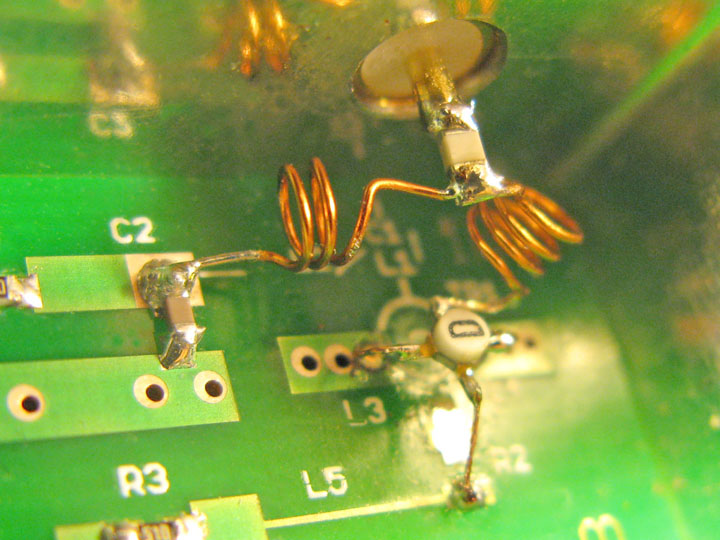 Fig. 4.5 Modified GaAs FET mounting
The result is shown in Figure 4.6. Improvement is 0.031 dB or 2.2K.
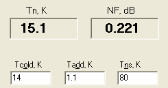 Fig. 4.6 Improved Noise Figure Test Results Step 3. Reducing the influence of the second stage.The LNA contains a number of elements intended to increase its stability but unfortunately they worsen the noise figure. For example resistor R3 (51 ohms), sitting in the DC part of the circuit adds a noticeable loss in the interstage circuit. This resistor degrades the noise figure of the second stage, and increases the overall noise figure. This effect was explained in the second part of the article. Let's try to remove the resistor.
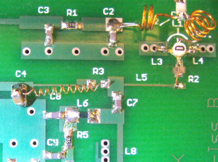 Fig. 4.7 Modifications to Interstage circuit
Figure 4.7 shows the modifications made with resistor R3 deleted. Instead of a resistor we used a choke coil, which goes to the blocking capacitor C4 (100 pF). Then a new 100 Ohm resistor goes to DC line at the old C4 location. The resistor and capacitor are soldered as an "air bridge" on the board. Thus resistor R3 (51 Ohm) is replaced by 100 Ohms. Previously we also removed resistor R2 (22 Ohms) and therefore, the total resistance is increased by 27 Ohms as compared to the original. The noise figure result of the alterations is shown Figure 4.8 and the improvement is 0.01 dB or 0.7K.
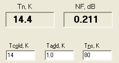 Fig. 4.8 Noise figure Results of Interstage modifications Step 4. Replacing the input connector.In order to minimize losses, the input circuit of LNA is directly connected to the input connector. Losses in the connector directly added to the noise figure. What could be bad about a beautiful shiny gold connector? The problem is that for the most of the connectors the thickness of gold plating is only 0.1 ... 0.2 microns. This is about 20 times smaller than the thickness of the skin layer. Under the gold it is always a layer of nickel, which serves as a barrier against the diffusion of gold in the lower layers. Below that the base metal of the connector is usually bronze, which is also a bad conductor and thus most of the high-frequency current flows through a poor conductor, which increases the losses. Thicker gold coatings are found only in expensive specialized connectors. But even there it is thinner than the skin layer at a frequency 1296 MHz. As a result, I started to use old Soviet silver plated connectors CP-50-727 whose silver plating of 6 microns is much more then the skin layer thickness and silver is the best conductor. For reference, the thickness of the skin layer at a frequency of 1 GHz in microns (10-6m) is: Silver 2.0
Copper 2.1
Gold 2.6
Nickel 9.0
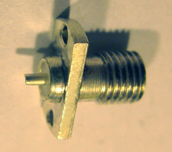 Fig. 4.9 Original CP-50-727 Input Connector
Figure 4.9 shows the CP-50-727 input connector in its original form. Then I cut off the excess and soldered it into place as shown in Figure 4.10.
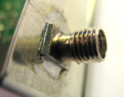 Fig. 4.10 Final Mounting of Modified CP-50-727 Connector
Results of connector replacement seen are seen in the Figure 4.11 and the improvement is 0.022 dB or 1.5K.
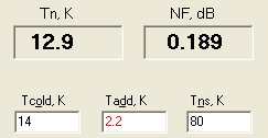 Fig. 4.11 Noise Figure Result after Input Connector Replacement Step 5. Replacing the input capacitor.I have not found in the specifications for the 2.7 pF input capacitor provided in the kit. Therefore, I decided to try to replace it by the already proven SQCAEA2R7BATME from AVX. This is critical element and a lot depends on it. Replacing the capacitor gave the result seen in Figure 4.12, and provides a further improvement of 0.01 dB or 0.7K.
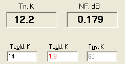 Fig. 4.12 Noise Figure Result with Input Capacitor Replacement Step 6. Replacing of the input transistor.The correct choice of the input transistor is a very important question. At first glance this step does not look complicated. You open the reference data and look for a transistor with very good noise figure at a frequency of 1300 MHz. But in practice, is not so easy. Experience shows that the best results are obtained on transistors, which are not intended to be used at such low frequencies. Often the data for the most interesting transistors is only shown starting from 2 or 4 GHz. But even if these data are given for the lower frequencies that we are interested in, the values given are only approximate. These results appear to be the result of mathematical modeling rather than actual measurements. Actual measurements used for production control are carried out at frequencies above 10 GHz, which is very far from our 23 cm band. All this complicates the correct choice of a transistor.
As a result, the only reliable method of choice is by direct experiment. Of course this is a very laborious method. Besides, if you test some type of transistor you never know what samples you got. For example I got poor results with ATF36077 and I do not know why I had a problem, but perhaps I did not obtain good samples of this transistor. Not all production runs give the same results. Another problem is counterfeiting, which is increasingly apparent in the world’s electronic components marketplace. Sometimes it is easy to identify counterfeit devices at a glance but often it is only determined by actual measurements.. Often there are accurate physically reproduced copies but internally these are low-grade transistors.
At first I got a really good noise figure result of close to 0.2 dB with a NE32584C transistor. Then I tried to find something similar using more modern NExxxxx transistors but no success. Despite the fact that the datasheet has promised good parameters, the real measurements did not confirm it. The next significant increase in sensitivity I got with using a MGF4919G. It is also not a new transistor and again I found that the modern MGF4953A was worse than the old device despite what was written in the reference data.
In October 2009, I checked my transistors in one of the latest versions of LNA. For each transistor was selected the optimum dc operating point and the input circuit also readjusted. I received the following noise figure results: FHX35 0.24 dB
NE32584C 0.22 dB
NE334S01 0.19 dB
NE3210S01 0.185 dB
NE3514S02 0.18 dB
NE3511S02 0.175 dB
MGF4953A 0.155 dB
MGF4919G 0.14 dB We must note that the measured sample of the NE32584C is obviously low quality but was recently purchased. The old ones which I purchased ten years ago are unfortunately all used up. For me at this moment the champion device is MGF4919G. All the other devices are also good, but the MGF4919G is the best.
With replacing the NE32584C with a MGF4919G there was a need to do some DC tuning and the final voltages at the gate was -0.155 V, and on the drain +1.2 V. Results of replacement are seen in the Figure 4.13 with an improvement of 0.028 dB or 2.0K.
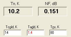 Fig. 4.13 Result of Replacing the NE32584C with MGF4919G Step 7. Replacing the inductor L2.Another source of additional noise at the input of LNA is a resistor R1 (51 ohms) in bias circuit of input transistor. The capacity of blocking capacitor C2 is small (8.2 pF), therefore resistor R1 adds noise to the input circuit. With decreasing frequency the losses created by R1 are increased, which ensures the stability of LNA at low frequencies. To reduce the losses at the operating frequency I decided to increase the inductance L2 from 2.5 turns to 4 turns. The input stage after this modification is shown in Figure 4.14.
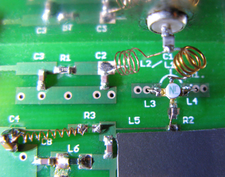 Fig. 4.14 Input Stage with Larger L2 coil
The results of this modification was an improvement of 0.008 dB or 0.5K as shown in Figure 4.15.
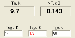 Fig. 4.15 Noise Result after Increasing L2 value Figure 4.16 and 4.17 show the swept measurement results after Step 7. Figure 4.16 shows the return loss from the input of the LNA. At a frequency of 1296 MHz it is 15.5 dB, which corresponds to the input VSWR = 1.4. The gain response of LNA is shown in Figure 4.17 and it is near maximum at1296 MHz with a value of 36.9 dB.
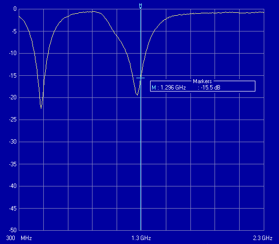 Fig. 4.16 Input Return Loss of the LNA
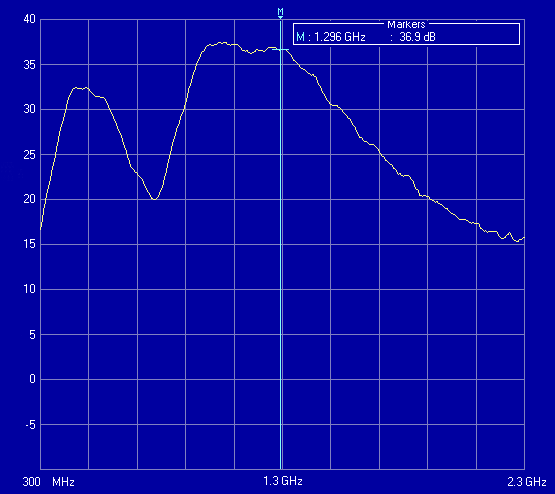 Fig. 4.17 Small Signal Gain Response And now the final step.
Step 8. Remove the C1 capacitor.
The input capacitor C1 really is not required for EME work. The probe of antenna feed has no DC contact with ground and it is well shielded from external influences. Therefore the electrical contact of transistor input with the antenna probe is totally safe. The problem is more with testing then in actual use of the LNA. The standard noise source has 50 ohms DC resistance on its RF port. So in this case we need additional DC block to be able to perform tests. Usually I use an SMA "male / female" DC Block type BLK-18 (Mini-Circuits) which has a blocking capacitor inside. For noise measurements with the "cold" horn antenna it is not a problem to remove the input capacitor since its input probe is also insulated from ground.
The modification made to remove C1 is shown on Figure 4.18. 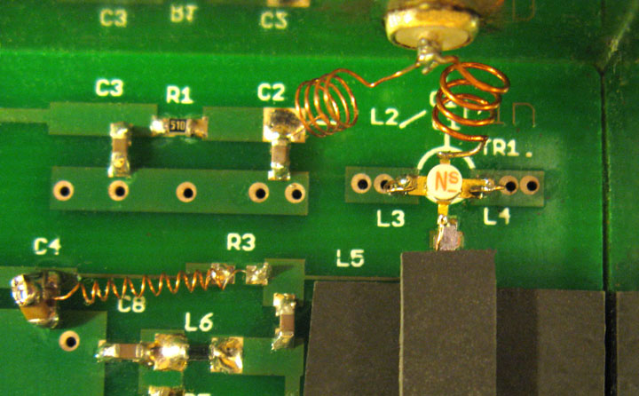 Fig. 4.18 Input stage with Input Capacitor C1 Removed Figure 4.19 shows in greater detail the wires in the source leads of the transistor that was discussed in Step 2. 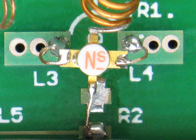 Fig. 4.19 Close Up of Source Lead Inductors Before this final step I tried to replace the MGF4919G with another one but it did not give a noticeable improvement. In contrast the removing of C1 gave the result shown in Figure 4.20 which improved the noise figure by 0.011 dB or 0.8 K. 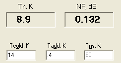 Fig. 4.20 Noise Result with Capacitor C1 Removed Summary and Conclusions. I have tried to demonstrate the effectiveness of the methods found in the course of numerous experiments. From time to time I used a modeling program, but more as a hint to guide my experiments and not as a main tool. I used the well tested 23 cm G4DDK preamplifier as a starting point with an amplifier that produced a 0.252 dB noise figure. All changes and improvements to this amounted to an improvement of 0.12 dB (or 8.4K), down to a final result noise figure of 0.132 dB (Tn = 8.9 K).
Since doing this work I have moved further forward and now have my own LNA design, which implements the demonstrated methods. But I'm still trying to improve it and I hope to finish this work soon and give a description of this LNA. My new LNA is still offers an improvement as compared with the actual test results shown here. The best noise figure that I have achieved is 0.125 dB. Thus far it is only an improvement of 0.007 dB (or 0.7K).
And, of course, recall that all these figures correspond to my own scale. Hundredths of a decibel are close to the true values. Thousandths of decibel are suitable only for relative measurements. |